Ps4 Motherboard Circuit Diagram
Ps4 pcb playstation teardown inside box game optical bottom drive Teardown: inside the playstation 4 game box Motherboard ps5
Inside the PlayStation 4: Motherboard Components Explained
Motherboard saa Jdm 055 schematic pcb Nec fic motherboard playstation
Inside the playstation 4: motherboard components explained
Jdm ps4 dualshock schematic circuit nummer circuito controladorTeardown: inside the playstation 4 game box Sony play station ps4 pro nva-001 power socket waysInside the playstation 4: motherboard components explained.
Voltage playstation standby nvg alzaabiJdm-055 (1-982-707-31) schematic Standby voltage diagrams alzaabiPlaystation 4 sad-003 (1-981-769-11) standby voltage diagrams by.

Playstation 4 nvg 001 standby voltage diagrams by alzaabi
Jdm 030 schematicTeardown inside pcb playstation box game antennas serving reveal chips module wifi visible artwork metal also cover off Ps5 digital hdmi port and mapped the traces that go to the filterPlaystation-4-motherboard-schematic ^new^.
Ps5 hdmi port filter gbatemp .


Jdm 030 Schematic

Playstation-4-motherboard-schematic ^NEW^

PlayStation 4 NVG 001 Standby Voltage Diagrams By ALZAABI - YouTube
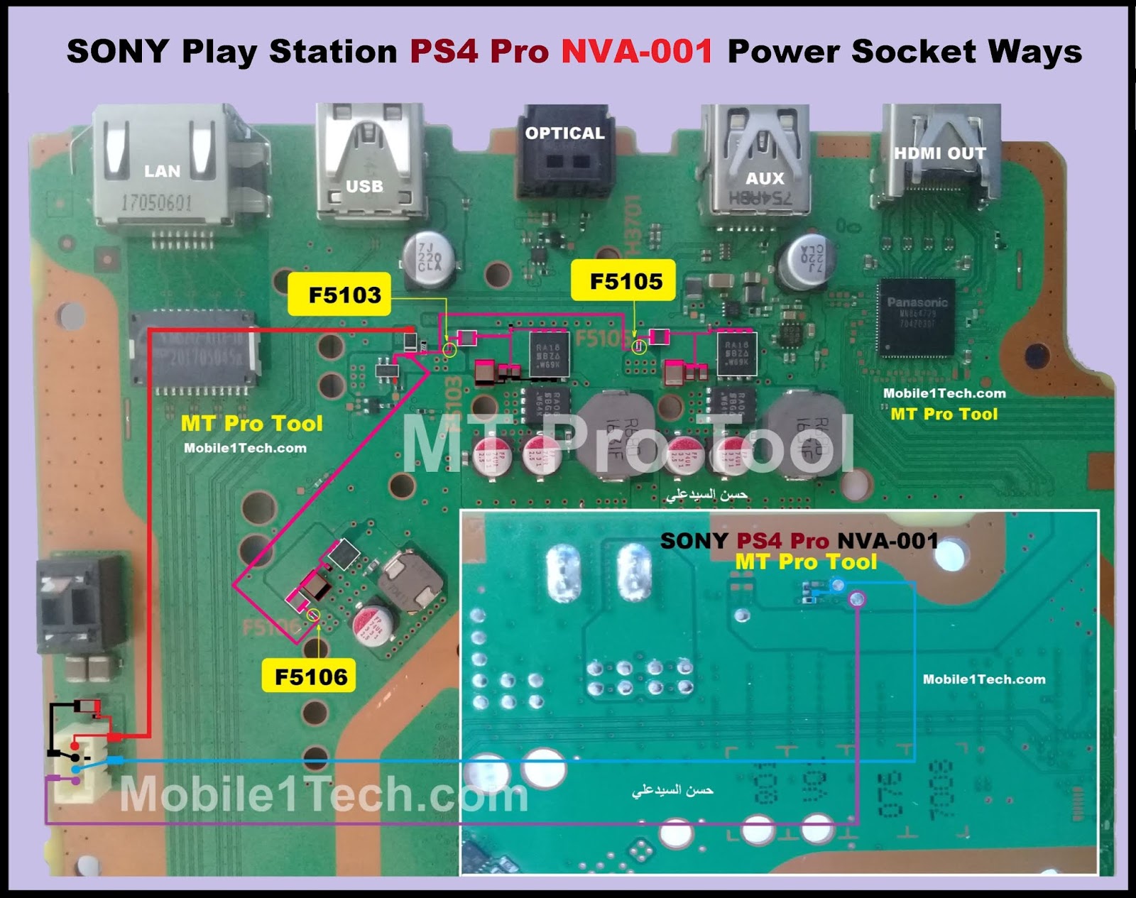
Sony Play Station PS4 Pro NVA-001 Power Socket Ways
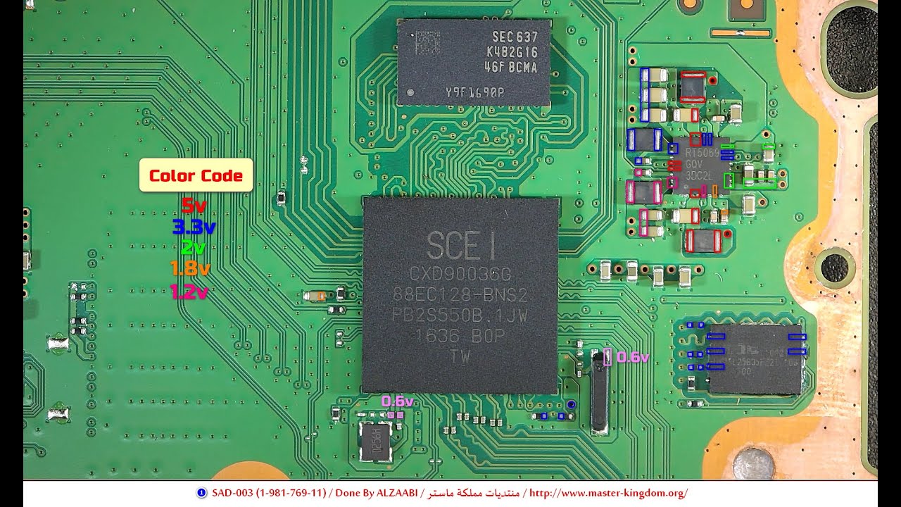
PlayStation 4 SAD-003 (1-981-769-11) Standby Voltage Diagrams By

Teardown: Inside the PlayStation 4 game box

Inside the PlayStation 4: Motherboard Components Explained

Teardown: Inside the PlayStation 4 game box

PS5 digital HDMI port and mapped the traces that go to the filter
